Offline
Melbourne, Australia
friendofmegaman wrote:

I'm not sure actually... this fragment (talking about GB RAM):

OK, that is talking about the address bus, which is 16-bit (64K), those are the addresses you use to write to / read from many different components in the GameBoy, it is not a break-down of what is stored in RAM.

Offline
Melbourne, Australia
friendofmegaman wrote:

Now I'm a bit confused are there two RAMs?

...right next to the CPU:

Offline
Boston, MA

rom is read from the cart as necessary, thats why games crash if you yank the cart out while playing. to my knowledge there are 2 sram chips in the gb, both 8kb, one for VRAM and one for the rest of the ram used by the cpu. if you only read the vram chip you'll only have access to tile and map data. i think you're right on other assumptions though, if you read both ram chips you should be able to use the data to assemble frames.. as long as the gb doesnt crash lol

Offline
CA

I see, so the RAM space is composed of VRAM and working RAM.
So it appears that CPU "sees" those two as a single chunk if data is that correct?
If so then when Arduino reads from the RAM we need to fix the addresses?

So from the implementation POV we're gonna need several shift registers (e.g. 8x8), two dual RAM chips.

Now I'm beginning to doubt is this idea really worth it. It's too much work to do for just video out... on the other hand I at least can comprehend it unlike FPGA that I have absolutely no idea about.

Anyways I'd like to see how's rvan's idea with shift registers before doing something that hardcore.
Also Nitro's suggestion seems easier to implement, so we should not be hasty here.

Offline
uXe wrote:
rvan wrote:

Good news.  But can the Arduino (or Teensy) access the RAM at 4.19 MHz, and when it is not providing the clock signal itself?  Clearly, we wouldn't have to read the RAM every single clock cycle, though.  Let's look more into whether the data stored in VRAM is in fact useful to us.

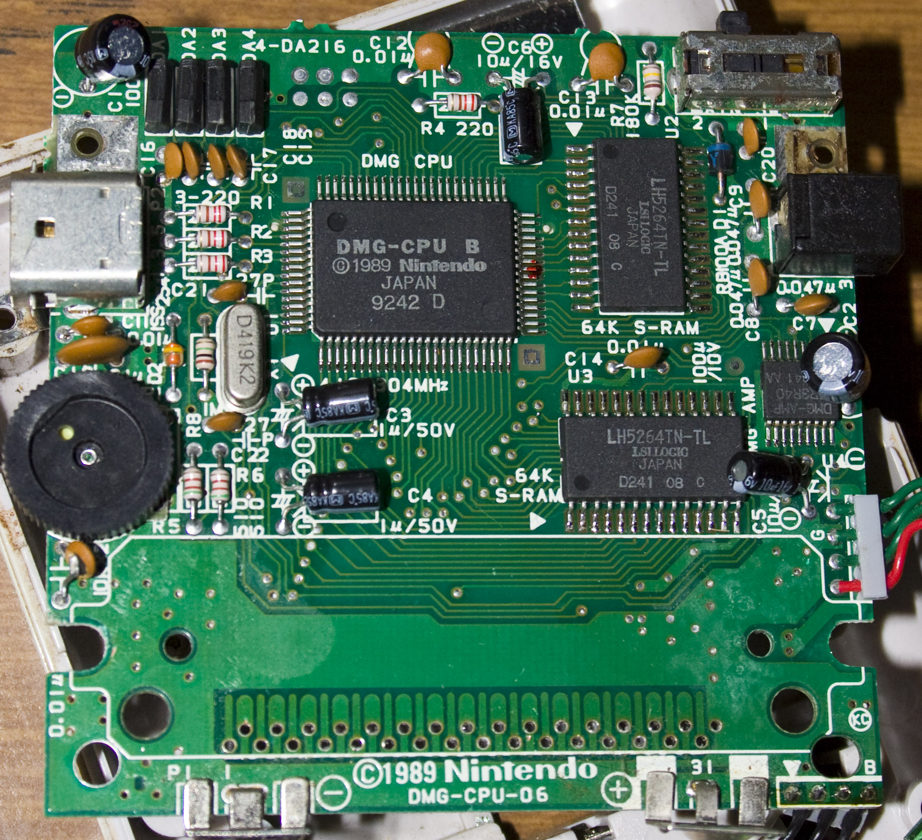
...it's SRAM (static) so it doesn't need to be clocked / refreshed the way DRAM (dynamic) does, here's a memory map:

I realize I wasn't entirely clear in what I was asking.  Rather, I was wondering whether the microcontroller would be able access the RAM while something else (i.e., the Game Boy), clocked at 4.19 MHz, was accessing it, as we would presumably have to access it between the Game Boy's read/writes.  It seems like the dual access SRAM solves this issue, though.

Other than the complexity of the RAM-snooping approach, my main concern is whether an Arduino/Teensy can in fact access the RAM as fast as the Game Boy updates it.  Does anyone have benchmarks for Arduino/Teensy RAM access?

Also, either bandwidth or processing power becomes a major issue here. We would either have to send all 8 kB of VRAM Data (+OAM etc.) every frame, or do enough processing on the microcontroller to work out which data we do need to send (which would amount to the MAP every frame and tile data + OAM when the tilebank is changed).  This is assuming whatever is running on the Game Boy is using sprites in a normal way.  The situation would be quite different for things like the Game Boy Camera and possibly LSDJ.

This does not seem the most viable approach for a computerless screen capture solution, which I am interested in in particular.

friendofmegaman wrote:

Any ideas how do we map the pins?

Pins marked A0-A12 on gameboy SRAM are mapped to either A0r-A12r or A0l-A12l

It seems like D0-D7 are mapped to IO0-IO7 (either r or l)

NOT OE also presented in both chips

This sounds right.  We would also connect the GB's /WR to the RAM's /R/Wx and /MOE to /OEx.  Incidentally, your image is of the DMG's system RAM rather than VRAM, but the two chips are the same type and the address and data buses are shared.  Also, uXe and ultramega are correct that we will need access to OAM, which is on the other SRAM.

friendofmegaman wrote:

So from the implementation POV we're gonna need several shift registers (e.g. 8x8), two dual RAM chips.

Why do we need shift registers here?  For accessing the two RAM chips from the microcontroller, can't we just invoke the relevant /CE line?

friendofmegaman wrote:

Now I'm beginning to doubt is this idea really worth it. It's too much work to do for just video out... on the other hand I at least can comprehend it unlike FPGA that I have absolutely no idea about.

Anyways I'd like to see how's rvan's idea with shift registers before doing something that hardcore.
Also Nitro's suggestion seems easier to implement, so we should not be hasty here.

Let's take a step back from everything here and think about what our overall aims for the project are, and what we can't achieve with an emulator or why we don't want to use an emulator.  Myself, I am interested in recording video (i.e., screen capture) from a DMG-01 with a device that is smaller than a SGB + SNES.

I am still going to try out my shift register idea and Nitro's idea next, when I find the time.

Offline
Melbourne, Australia
rvan wrote:

Also, either bandwidth or processing power becomes a major issue here. We would either have to send all 8 kB of VRAM Data (+OAM etc.) every frame, or do enough processing on the microcontroller to work out which data we do need to send (which would amount to the MAP every frame and tile data + OAM when the tilebank is changed).  This is assuming whatever is running on the Game Boy is using sprites in a normal way.  The situation would be quite different for things like the Game Boy Camera and possibly LSDJ.

This does not seem the most viable approach for a computerless screen capture solution, which I am interested in in particular.

The three-pixels-per-byte approach would still mean having to send 7.5kB every frame anyway, not that big a difference.

I do agree though that it would become a little complex, may be it could be an idea for the folks who are making plans to produce brand new motherboard PCBs to include dual-port SRAMs on them though! smile

rvan wrote:

I am still going to try out my shift register idea and Nitro's idea next, when I find the time.

Good to hear, looking forward to the results!

Offline
CA

rvan could you share a bit more about your shift register approach?
Concretely I wonder how did you wire the pins:

Q0 - Q7 -> Teensy
GND, Vcc -> GND, +5V
Q7S - I guess not connected or grounded?
MR - ?
SHCP -> LCD CLOCK?
STCP - what's the role of the storage clock?
OE  - ?
DS -> Data0 / Data1

How do you know when it's time to read data from the register?

Also I was theorizing on how this would work out. Since we can read a byte in one go we're reading with roughly 500KHz and we have 96M/500K = 192 cycles are left to shoot data to PC. So in theory looks legit. Especially if combined with Nitro's approach it might be super neat.

Another question I have is how do we produce clock signal with Arduino / Teensy?

Offline
Melbourne, Australia
friendofmegaman wrote:

Now I'm a bit confused are there two RAMs?

...at the risk of flogging a dead horse, the GameBoy Color and GameBoy Pocket only have a single SRAM onboard - so we'd be back to just the one dual-port SRAM to make it work:


http://console5.com/wiki/SRAM_64Kb:_8K_x_8-bit


http://console5.com/wiki/SRAM_256Kb:_32K_x_8-bit

Edit: unless the VRAM is built into the CPU? hmm

Edit: Yep... (from http://www.docstoc.com/docs/48266995/CGB-Service-Manual)

Last edited by uXe (May 10, 2014 4:20 am)

Offline
uXe wrote:

The three-pixels-per-byte approach would still mean having to send 7.5kB every frame anyway, not that big a difference.

You're right.  I was thinking of four pixels per byte when I did the calculations.

uXe wrote:

I do agree though that it would become a little complex, may be it could be an idea for the folks who are making plans to produce brand new motherboard PCBs to include dual-port SRAMs on them though! smile

That's a great idea re the new boards.

friendofmegaman wrote:

rvan could you share a bit more about your shift register approach?

Well, the shift register approach didn't work out, although the code ended up being simpler than I expected.  It seems that the Teensy can't keep up, even when the data is coming in eight times slower.  Everything works until I store a byte of data in the array.  It seems this must be too expensive an operation.

Nonetheless, here is the code.  Wiring is in the comments.  Hopefully this answers your questions.  Let me know if it doesn't and I can elaborate further.

//Author: rvan
//Read 8-bit parallel data from a shift register and send it over the USB
//Serial.  DOES NOT WORK, as storing a byte in the line array is too slow.

/*
     DMG    4017       74HC595    MK20DX256VLH7
     CLK    CLK        SRCLK
            DO8->RST
GND         CE
            DO1        RCLK       PTB0
     D0                SER
GND                    /OE
VCC                    /SRCLR
                       QA         PTC0
                       ..         ..
                       QH         PTC7
*/

#include <WProgram.h>

volatile int i = 0;
uint8_t line[20]; //Using uint8_t here doesn't make any difference.

//These contain the contents of the GPIO register to which the clock
//divider's output is connected to pin zero of.
uint32_t shclk_prev, shclk = 0;

int main() {
    for(i=0;i<=23;i++) {
    //We set all the pins (including those we don't care about) to inputs.
    //We don't know why GPIOx_PDDR doesn't seem to do anything.
        pinMode(i, INPUT);
    }
    i = 0; //For reuse.
    pinMode(16, OUTPUT); //PTB0

    for(;;) {
        //Bitmask is necessary because other lines will be floating.
        shclk = GPIOD_PDIR & 0b1;
        if(shclk_prev==1 && shclk==0) {
            GPIOB_PTOR = 0b1; //Debug, toggle output.
            //This line is the problem.  If we leave it out, PTB0 toggles as
            //expected.
            line[i] = GPIOC_PDIR;
            i++;
        }
        shclk_prev = shclk;
        /*
        if(i==20) {
            Serial.write(line, 20);
            i = 0;
        }
        */
    }
}
friendofmegaman wrote:

Another question I have is how do we produce clock signal with Arduino / Teensy?

Although we saw that the DMG's clock crystal produces a sine wave, I am not convinced that this waveform is necessary for the CPU's clock, given that neither the LTC6930 (Kitsch-Bent's easy_CLK) nor the LTC1799 produces a sine wave.  Synthesizing a square wave (which should in theory work fine) is as simple as toggling a digital output pin (other waveforms are more CPU intensive).

Edit: Fixed wiring layout indentation.

Last edited by rvan (Jun 2, 2014 12:32 am)

Offline
CA

Thanks for sharing rvan!

rvan wrote:

Although we saw that the DMG's clock crystal produces a sine wave, I am not convinced that this waveform is necessary for the CPU's clock, given that neither the LTC6930 (Kitsch-Bent's easy_CLK) nor the LTC1799 produces a sine wave.  Synthesizing a square wave (which should in theory work fine) is as simple as toggling a digital output pin (other waveforms are more CPU intensive)

Doesn't work for me...

Offline
friendofmegaman wrote:

Doesn't work for me...

Post your code!

Offline
Melbourne, Australia

Found this nice helpful document:

http://students.washington.edu/fidelp/g … Manual.pdf

Which shows that the OAM (Sprite) RAM is actually internal to the CPU:

So that puts a damper on the dual-port RAM approach, unless you use a hack to mirror $FE00-$FE9F into some 'unused' VRAM and read it from there... Still, there would be much fun to be had playing around with dual-port SRAMs and reading / writing the GameBoy's memory aside from video! smile

PS. the above PDF also provided this helpful diagram:

Offline
Boston, MA

doh! this is an interesting read smile

Offline
CA
rvan wrote:
friendofmegaman wrote:

Doesn't work for me...

Post your code!

Sure, sorry guys I'm just loaded with work lately so things keep slipping off my mind. Here's the code (I know Jazz won't approve):

(Teensy only, won't work on Arduino)
Timer based

const int pClk = 10;
int clk_state = LOW;
IntervalTimer myTimer;

void setup(){
    pinMode(pClk, OUTPUT);
    // I played with the timeout - no lucj
    myTimer.begin(tick, 0.125);
}

void tick(){
  if(clk_state==LOW)clk_state = HIGH;
  else clk_state = LOW;
  digitalWrite(pClk, clk_state);
}
Offline
CA

Some thoughts on further steps:

1. Remember my suggestion about webcam based approach? Well it looks like all the web cams are 30fps and GB is 60 fps so it's not an option. There are probably some faster web cams but they're expensive.

2. I PM'ed Nitro about clock master and here's how he'd go about it:

Nitro2k01 wrote:

You need a loop, where you do something like the following. This assumes digital pin 0 is connected to the clock input of the Gameboy.

PORTD |= 1; // Turn on clock signal
(Wait a little and/or do something.)
PORTD ^= ~1; // Turn off clock signal
(Wait a little and/or do something.)

PORTD ^= 1; // Flip clock signal (xor)
(Wait a little and/or do something.)
PORTD ^= 1; // Flip clock signal (xor)
(Wait a little and/or do something.)

If done perfectly, you now get a perfect square wave output. It does not have to be perfect, but...
1) It can't be too fast, or the CPU or cartridge maybe will not be able to do everything it needs before the next clock pulse arrives.
2) A little deviation from the correct clock frequency is tolerable, as long as the long term average is correct. For example, you might send a slightly too slow clock during the period when the data is being sent and a slightly too fast clock during the blanking periods when no data is transmitted. Even though the CPU itself is fine with a slightly varying clock, the audio output may get artifacts from this, like maybe a buzzing or FM type effect.

However he also mentions that he's not sure if after all it can help us to get the video and we gonna need to use assembly. That's a bit discouraging, but ok, let's keep this in mind.

3. FPGA. I personally like this option because at least I'm sure it CAN be done with FPGA. However I have no idea how big a board we gonna need for that (how big = how expensive). A good powerful board (that will most certainly do the thing) will cost around $150. I'd buy one if have no other choice, but at the moment it's cheaper to buy an SNES or its clone and tear it apart and use SGB.

5. VRAM - uXe posted that it is hardly doable (although a number of other things can be done with this approach, so the idea is still brilliant IMO).

Other thoughts.

Now let's look one more time at what we're facing.

- It's a 4MHz (rough estimate, I don't count dead time) 5-channel data flow.
- Even with 2GHz uC (let's assume one exists) we'll have 500 cycles to monitor 5 channels and send data to PC as fast as 4Mbs (or if we're assembling the frame in uC then 2,7mbs but then we need cycles to assemble the frame).
- Even making uC a clock master - we have predictable timing BUT it's still 4M just more precisely measured.

Looks pretty bad now. The only one cheap enough viable option is using SGB. What I don't like about this approach (and rvan has already mentioned this) is that we end up with the de-digitized signal that we'll have to re-digitize. It will work, but it's like turning your night lamp via Internet through a proxy in China (unless you're in China but then replace China with USA).

Apart from that it's either FPGA or some cam-corder type. Thoughts?

Last edited by friendofmegaman (May 6, 2014 9:53 pm)

Offline
Melbourne, Australia
friendofmegaman wrote:
rvan wrote:

Post your code!

Sure, sorry guys I'm just loaded with work lately so things keep slipping off my mind. Here's the code (I know Jazz won't approve):

(Teensy only, won't work on Arduino)
Timer based

const int pClk = 10;
int clk_state = LOW;
IntervalTimer myTimer;

void setup(){
    pinMode(pClk, OUTPUT);
    // I played with the timeout - no lucj
    myTimer.begin(tick, 0.125);
}

void tick(){
  if(clk_state==LOW)clk_state = HIGH;
  else clk_state = LOW;
  digitalWrite(pClk, clk_state);
}

Well, your tick routine could be simplified down to just a single GPIOx_PTOR command to toggle the pin state, but even then I don't think the interrupt is going to be fast enough to get back in time to toggle it again 125 nanoseconds later!

Maybe direct control over the clock would be easier to achieve by having the microcontroller generate a variable signal that can be fed into the standard variable clock mod chip (what the potentiometer normally does - not sure if it is wired as a voltage divider or a variable resistor though?) as well as start / stop control over the clock mod - at least then there would be predictability?