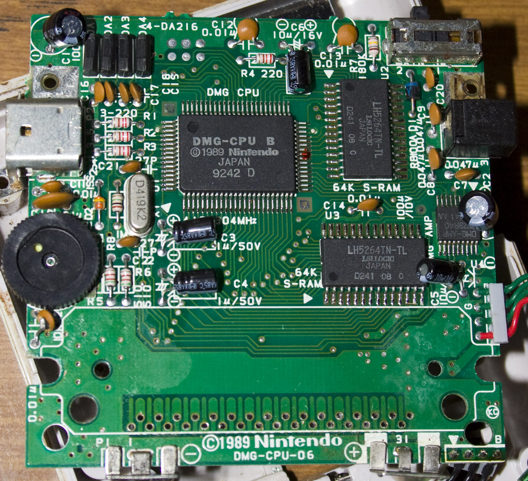
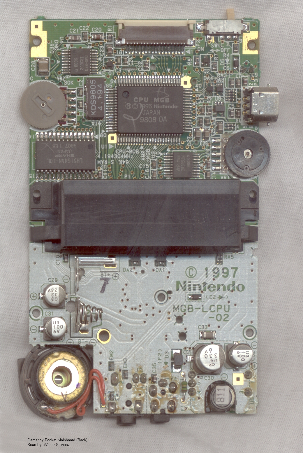
uXe wrote:rvan wrote:Good news. But can the Arduino (or Teensy) access the RAM at 4.19 MHz, and when it is not providing the clock signal itself? Clearly, we wouldn't have to read the RAM every single clock cycle, though. Let's look more into whether the data stored in VRAM is in fact useful to us.
...it's SRAM (static) so it doesn't need to be clocked / refreshed the way DRAM (dynamic) does, here's a memory map:
I realize I wasn't entirely clear in what I was asking. Rather, I was wondering whether the microcontroller would be able access the RAM while something else (i.e., the Game Boy), clocked at 4.19 MHz, was accessing it, as we would presumably have to access it between the Game Boy's read/writes. It seems like the dual access SRAM solves this issue, though.
Other than the complexity of the RAM-snooping approach, my main concern is whether an Arduino/Teensy can in fact access the RAM as fast as the Game Boy updates it. Does anyone have benchmarks for Arduino/Teensy RAM access?
Also, either bandwidth or processing power becomes a major issue here. We would either have to send all 8 kB of VRAM Data (+OAM etc.) every frame, or do enough processing on the microcontroller to work out which data we do need to send (which would amount to the MAP every frame and tile data + OAM when the tilebank is changed). This is assuming whatever is running on the Game Boy is using sprites in a normal way. The situation would be quite different for things like the Game Boy Camera and possibly LSDJ.
This does not seem the most viable approach for a computerless screen capture solution, which I am interested in in particular.
friendofmegaman wrote:Any ideas how do we map the pins?
Pins marked A0-A12 on gameboy SRAM are mapped to either A0r-A12r or A0l-A12l
It seems like D0-D7 are mapped to IO0-IO7 (either r or l)
NOT OE also presented in both chips
This sounds right. We would also connect the GB's /WR to the RAM's /R/Wx and /MOE to /OEx. Incidentally, your image is of the DMG's system RAM rather than VRAM, but the two chips are the same type and the address and data buses are shared. Also, uXe and ultramega are correct that we will need access to OAM, which is on the other SRAM.
friendofmegaman wrote:So from the implementation POV we're gonna need several shift registers (e.g. 8x8), two dual RAM chips.
Why do we need shift registers here? For accessing the two RAM chips from the microcontroller, can't we just invoke the relevant /CE line?
friendofmegaman wrote:Now I'm beginning to doubt is this idea really worth it. It's too much work to do for just video out... on the other hand I at least can comprehend it unlike FPGA that I have absolutely no idea about.
Anyways I'd like to see how's rvan's idea with shift registers before doing something that hardcore.
Also Nitro's suggestion seems easier to implement, so we should not be hasty here.
Let's take a step back from everything here and think about what our overall aims for the project are, and what we can't achieve with an emulator or why we don't want to use an emulator. Myself, I am interested in recording video (i.e., screen capture) from a DMG-01 with a device that is smaller than a SGB + SNES.
I am still going to try out my shift register idea and Nitro's idea next, when I find the time.


