from the EAGLE Manual
"
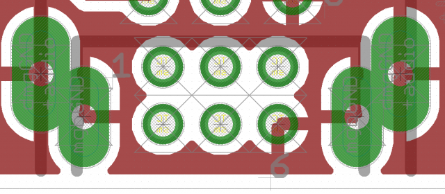
8.11 Components with Oblong HolesIf the board manufacturer have to mill oblong holes, you have to draw the
milling contour of oblong holes in a separate layer. Usually this is layer 46, Milling.The milling contour for components that need oblong holes can be drawn
with WIRE (and possibly ARC) with a very fine wire width near or even 0 in the Package Editor. Take a pad that has a drill diameter which lies inside the milling contour, or SMDs, for example in Top and Bottom layer, as basis for the oblong hole.In case of a multilayer board you should draw a WIRE in the used inner
layers at the position of the oblong holes so that it covers the milling contour and leaves a kind of restring around the opening.Please inform your board manufacturer that they have to take care on the
milling data drawn in this layer. Also tell them whether they should be
plated-through or not.
"hope that helps! its not too bad.
you all may also want to create a custom library called "oblong holes" if you have a need of them individually (rather than as a part's footprint). its a time saver
Nice! Thanks, Matt! It only sounds slightly easier than my method. An oblong library is a good idea though! I wouldn't be surprised if there is already one out there.
Last edited by thursdaycustoms (Mar 8, 2014 5:53 pm)