bit 9 wrote:
thursdaycustoms wrote:I'm a complete Eagle CAD addict!
Ok, so let me pick your brain for a moment. How on earth do you make oblong through-holes? I'm doing unspeakable things with layers to get the battery contact points, DC jack, switch, and link port to look right. Part of my reluctance of releasing the file is that whole 'there has to be a better way to do this' thought.
Oblong holes are very annoying when you intend the rest of the pads to be round.
Here's how I do it. I'm no expert, just an addict so there could be a better way. This is just the method I've come up with:
-Drop a through hole pad.
-Draw a line using the "Pads" layer that is just a little bit wider than your original pad or however wide you want it to be.
-Use the "Dimension" layer to draw your oblong hole at zero width(make sure it's slightly wider than the drill of the pad or it will be really wonky).
-Then use "tStop" and "bStop" layers to expose the copper.
-You may need to use "tRestrict" and "bRestrict" since it recognized the "Dimension" line as an edge of the PCB.
-If you had to use the "restrict layers then you will have draw lines to the pads for the thermal. If they don't connect on the trace you want then just use the Name command to add it to the line.
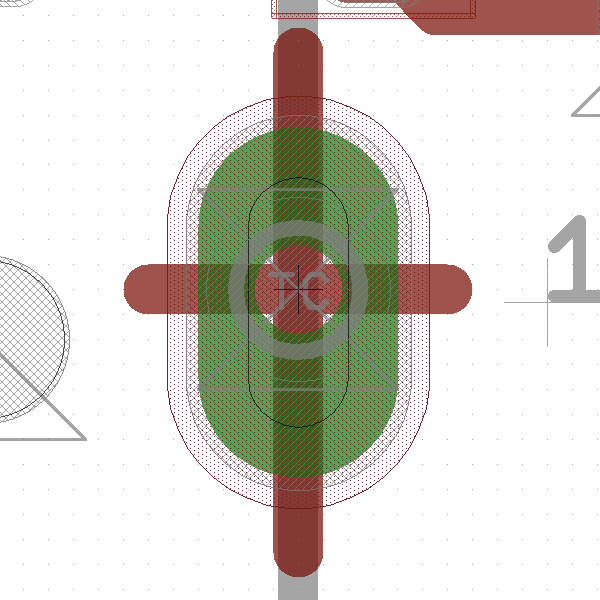
Here is what my oblong pad looks like after all that hard work:

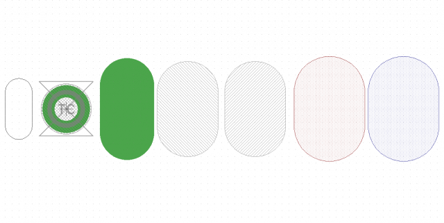
Here are the individual layers/parts not including the lines:

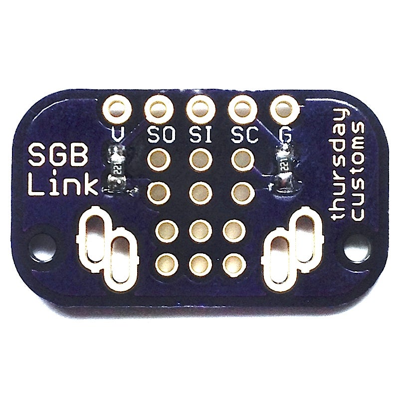
And here's how they turned out in some of my kits:


I hope this helps! Let me know if you have any questions on this.
If anyone knows of an easier way I would be glad to hear it! But if not I do like the degree of control I get here for every individual layer. You could also make your own part.. But I always found that to be more annoying than this method.
